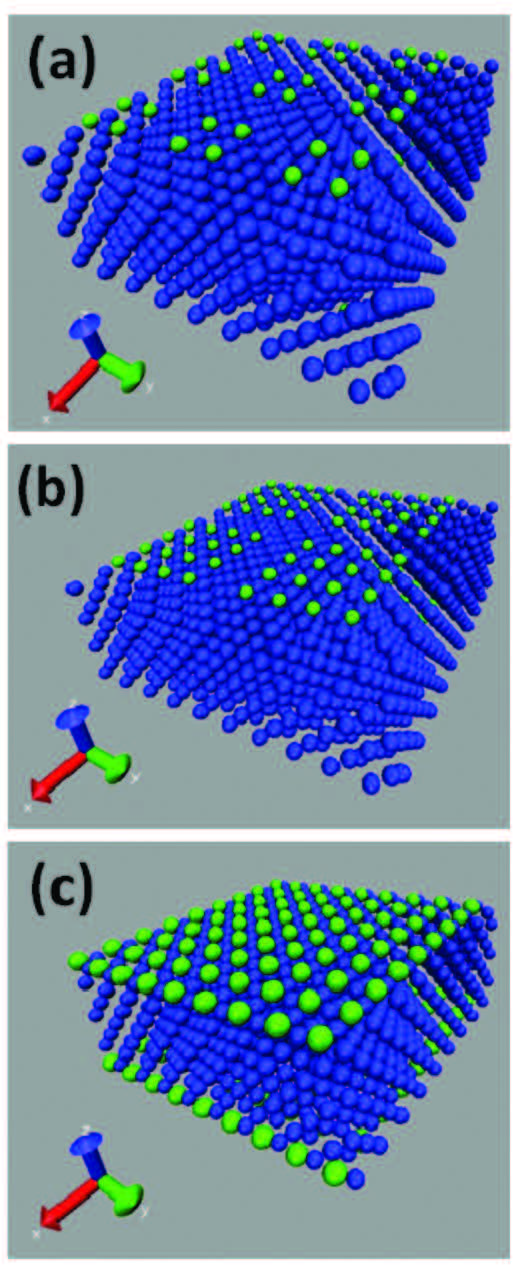
Atomic models of (a) a 2x2 island, (b) a 4x4 island, and (c) a monolayer of N atoms on Cu [001].
Surprising behaviors often arise when small numbers of atoms and molecules are brought into close proximity. Such small aggregates offer a window into an intermediate state of matter between isolated atoms and bulk materials. An improved understanding and control of these nanometer-scale structures may contribute to new paradigms for technologies such as molecular circuits, spin-based electronics and quantum computation.
A research team led by Ohio State University’s Jay A. Gupta, assistant professor of physics, and David G. Stroud, professor of physics, is using scanning tunneling microscopes (STM) to better measure the properties of nanoscale structures, whose size can vary from a few atoms to thousands of atoms.
Quantum confinement of electrons in the cluster leads to a discrete spectrum of states with a level spacing that depends on the size. By isolating the nanocluster from the underlying metal substrate by using an ultrathin insulating film of only a few atomic layers (e.g., Cu2N islands), scientists can measure this spectrum with STM. They seek to understand how these electronic structure properties depend on the dimensions of nitrogen islands.
“We have studied the electronic structure of nanoscale islands of Cu2N on the Cu [001] surface,” said Gupta. “We leverage hundreds of processors on Ohio Supercomputer Center systems to perform ab-initio calculations using density functional theory. Those results are compared with our scanning tunneling microscopy measurements, and we find that our tunneling spectroscopy results are in good agreement with our computational predictions.”
--
Project lead: Jay Gupta, The Ohio State University
Research title: Emergence of band structure in nitrogen islands on copper [001]: Comparison of
density functional theory and scanning tunneling microscopy
Funding source: Center for Emergent Materials - The Ohio State University