Ohio State University researchers recently discovered potential keys to mass producing a specific pattern of graphite in a layer just one atom thick, signaling a breakthrough that could lead to “graphene” challenging silicon as the preferred material for manufacturing faster, more efficient computer chips.
While scientists have known of graphene’s potential for many years, electronics industry officials became particularly excited when researchers found that thin layers of graphite are highly stable, visible under the right conditions even when only one atom thick, stronger than steel and conducts electricity quickly and in exceptional ways.
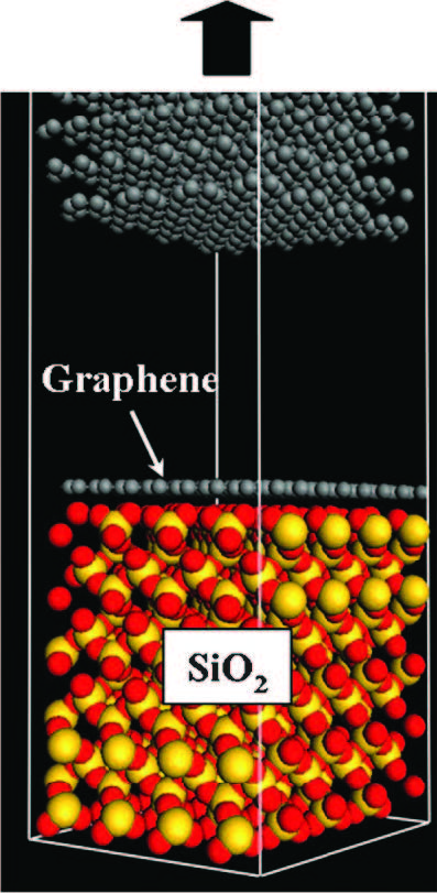
Wolfgang Windl, Ph.D., associate professor of Materials Science and Engineering, and co-workers set out to develop a method for producing very accurate, very positionspecific graphene patterns in a way that industry could use to manufacture computer chips. To test their technique, Windl turned to the resources of the Ohio Supercomputer Center and the Vienna Ab-initio Simulation Package.
“The calculations are computationally very demanding for the systems under consideration due to their size and complexity,” Windl explained. “Based on our initial success with these computer simulations, we currently model adhesion on different substrates along with the resulting electrical transport through the graphene to optimize the stamping process and the resulting devices.”
With confirmation from their computer models, Windl’s team from OSU’s Center for Emergent Materials successfully sheared off graphite layers that were about ten atomlayers thick and have initiated the process of obtaining a patent on the technique.
--
Project lead: Wolfgang E. Windl, The Ohio State University
Research title: Toward site-specific stamping of graphene
Funding sources: National Science Foundation, The Ohio State University